What is Moore’s Law?
Gordon E. Moore …..who was co-founder of both Fairchild Semiconductor, and Intel Corporation……played a pivotal role in developing the ‘printing’ process….by which the first successfully marketed integrated circuits…were mass-produced.
Moore was Director of Research and Development at Fairchild, when he first made the observation, that we now call ‘Moore’s Law’
In 1965, in an article in the trade journal, Electronics, he summarized his observations of the exponential growth in the density of transistors on silicon wafer.
Because Moore’s Law is slowing down…..researchers are exploring many possible ways that the exponential growth in technological evolution might continue.
What are the Limitations Causing Moore’s Law to Slow Down?
slowing down — due to heat
limitations on transistor size
quantum tunneling – Leakage current between two metal transistor electrodes results when the gap between the electrodes narrows to the point that electrons are no longer contained by their barriers — a phenomenon known as quantum tunneling.
The quantum tunneling effect is a quantum phenomenon which occurs when particles move through a barrier that, according to the theories of classical physics, should be impossible to move through.

What New Frontiers Will Allow Us to Transcend the Limitations in Moore’s Law?
- ) graphene transistors – conduct electricity more easily; increase clock speed
- ) 3-dimensional chips – using carbon nanotubes
- ) molecular transistors – first created in 2009
- ) photon transistors
- ) quantum computers – good for parallel processing
- ) protein computers
- ) DNA computers
Computer-aided detection (CAD) is a well known example of machine learning
The driving force of technological change, in medical imaging, is interactive holographic systems (IHS), a combination of stereo and virtual holography that allows the user to work with objects in 3D/4D open space as well as with standard images (2.5D).
“At our site, the total number of images the radiology department must interpret on a daily basis has doubled every 4.5 years. “
Biomedical Engineering Domains:
Diffusion-weighted magnetic resonance imaging (DWI or DW-MRI) is the use of specific MRI sequences as well as software that generates images from the resulting data that uses the diffusion of water molecules to generate contrast in MR images.[

ULTRASOUND IMAGING:
There were three main drivers pushing ultrasound imaging technology toward functional and volume imaging, namely, increased computational power, the trend toward cost-effective volume imaging and the availability of contrast agents for ultrasound imaging.
ultrasound: 1) Moore’s Law-reduction in size of electronics 2) ASICs:application specific ICs
3) DSP chips- digital signal processing chips
4) Higher speed computing (hardware….software)
——sonosite: portable ultrasound
——–2007: Siemens: pocket ultrasound
Philips: Lumify app….plugs into ‘smart phone’: The system consists of a Lumify transducer, which connects to the app via USB connection. There is a companion app available for Android devices and is free of charge. There is a list of compatible devices available that includes cell phones and tablets.
Butterfly Network: put entire ultrasound on a chip: “This incredible piece of technology is like having multiple transducers in one easy to use handheld device. True whole-body imaging in one device, and viewed on an iPhone or iPad. You can go to a case, have immediate boot-up, perform your sonogram, and if needed, share your images for immediate consultation. The images are high-quality. Unlike conventional ultrasound technology, where transducers have fixed abilities, programming can be performed to continue improving the Butterfly images.
COMPUTERIZED TOMOGRAPY:
Driven by the clinical benefits, manufacturers have improved the performance of CT scanners at an impressive rate, equivalent to a form of “Moore’s Law” with performance doubling every 25 months for over 30 years.
include image-guided therapy for the interventional radiologist and surgeon using multimodality hybrid imaging technologies. Such devices that are discussed include CT-integrated robotic systems for percutaneous needle insertion, electromagnetic tracking for laparoscopic positional correction, and fusion of live ultrasound imaging with CT datasets. The goal of these devices would allow image-based treatment planning, guidance, monitoring, and controlling of treatment effectiveness
One approach to extending Moore’s Law involves the new ‘Chemistry-based Data Storage‘
“In this case, hardware, including transistors, will conceivably fit on individual molecules, reducing chip sizes much more significantly than Moore ever envisaged. “

Scientists use carbon nanotubes to make the world’s smallest transistors
. For electronic equipment, especially medical imaging systems, this doubling of processing power also implies greater availability of network bandwidth, larger storage capacity, smarter computer algorithms, and better understanding of clinical information.
tensor cores; tensor sort

In mathematics, a tensor is an algebraic object that describes a linear mapping from one set of algebraic objects to another. Objects that tensors may map between include, but are not limited to, vectors and scalars, and, recursively, even other tensors (for example, a matrix is a map between vectors, and is thus a tensor.
Mathematically speaking, tensors are more than simply a data container, however. Aside from holding numeric data, tensors also include descriptions of the valid linear transformations between tensors.
graphene transistors – conduct electricity more easily; increase clock speed – A cascading series of graphene transistor-based logic circuits could produce a massive jump, with clock speeds approaching the terahertz range – a thousand times faster.
3-dimensional chips – using carbon nanotubes – [rolled-up sheets of carbon atoms just 1 nanometer, or a billionth of a meter, in diameter.]
molecular transistors – first created in 2009
photon transistors:
Now, researchers at the University of Maryland’s A. James Clark School of Engineering and Joint Quantum Institute (JQI)—led by Professor of Electrical and Computer Engineering, JQI Fellow, and Institute for Research in Electronics and Applied Physics Affiliate Edo Waks—have cleared this hurdle and demonstrated the first single-photon transistor using a semiconductor chip.
Researchers build an all-optical transistor
An optical switch that can be turned on by a single photon could point toward new designs for both classical and quantum computers.
2013 – MIT – first optical transistor – beams of light

quantum computers – good for parallel processing
protein computers:
The ‘biocomputer’ uses a similar strategy to that of quantum computers, using qubits – or the quantum computing equivalent to bits. But the qubits are replaced with short strings of living proteins, as well as molecular motors called myosin which are used in living things to carry out mechanical tasks in living cells, to move the protein filaments along artificial paths.
DNA computers – DNA-based logic gates that could carry out calculations inside the body have been constructed for the first time.
2012 – team at Harvard
FinFET = Fin-shaped Field Effect Transistor – reduces leakage due to quantum tunneling
GAAFET -‘Gate all around Field Effect Transistor’

uses silicon nanosheets – That transistor design goes by a variety of names—gate-all-around, multibridge channel, nanobeam—but in research circles we’ve been calling it the nanosheet.
expected to come to market – 2021-2023
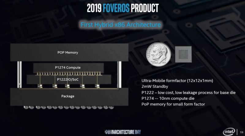
Intel: Foveros – stacking ‘chiplets’ and memory on top of each other

EMIB – Embedded Multi-die Interconnect Bridge – In 2019, Intel began to ship chips using a new 3D stacking technology the company is calling Foveros. Foveros allows complex logic dies to be stacked upon one another, providing a much greater ability to mix and match processor components with optimal manufacturing processes.
deep learning – machine learning
-training depends on a large amount of data
- -requires massive amounts of computational resources [cloud computing]
“:”accelerators”
chiplet, die, node, multi-chip module
‘multiwave imaging’ – photoacoustics: recent breakthroughs in optics have shown that coherent light propagating through optically scattering medium could be manipulated towards novel imaging approaches.
plane wave – fast imaging
shear wave elastography
nanomagnetic logic – (NML) is a “beyond-CMOS” technology that
uses bistable magnets to store, process, and move binary information.
Dannard Scaling
Amdahls law
Neural Algorithm
Many applications such as radio frequency (RF) devices, power management subsystems, passive components, biochips, sensors, actuators, microelectromechanical systems (MEMS) play an equally important role in today’s semiconductor products. Integrating analog functions into CMOS-based specialty technologies enables cost-optimized and value-added system solutions. These diversified technologies are known as “More than Moore.”
REFERENCES:
https://www.diagnosticimaging.com/practice-management/moores-law-medical-imaging
https://i.ytimg.com/vi/dQoW6P1JWLE/maxresdefault.jpg
https://www.extremetech.com/wp-content/uploads/2018/12/Foveros-3.jpg
https://www.xfab.com/about-x-fab/more-than-moore/what-is-more-than-moore/
https://phys.org/news/2018-07-semiconductor-quantum-transistor-door-photon-based.html